
產品專區
- Hiden Analytical
- Electrochemistry DEMS
- FIB-SIMS-聚焦離子束二次離子質譜奈米材料分析系統
FIB-SIMS-聚焦離子束二次離子質譜奈米材料分析系統
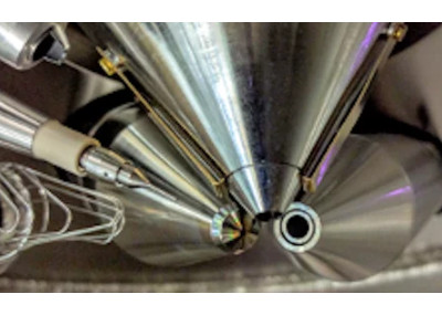
FIB-SIMS-聚焦離子束二次離子質譜奈米材料分析系統
為既有 FIB 系統增加高靈敏度 SIMS、奈米級 Elemental Mapping 與 3D Depth Profiling
Hiden FIB-SIMS 是一套可整合至既有 Focused Ion Beam(FIB)系統的高性能 Secondary Ion Mass Spectrometry 分析方案。
系統結合 FIB 的精密 Primary Ion Beam 與 SIMS 的高表面靈敏度,可對材料最上層奈米區域進行 Elemental、Isotopic、Atomic Ion 與 Molecular Ion Analysis。
此架構特別適合先進材料、半導體、薄膜、電池與奈米科技中的高靈敏度表面 Mapping、Depth Profiling 與 Correlative Microscopy。
FIB-SIMS 系統概述
結合 Focused Ion Beam 與 Secondary Ion Mass Spectrometry,提供奈米尺度高靈敏度化學分析。
FIB 可將 Primary Ion Beam 聚焦至極小區域,並利用受控 Sputtering 移除材料。當 Primary Ion Beam 轟擊 Sample Surface 時,材料會產生 Secondary Ions。
FIB-SIMS 收集並分析這些 Secondary Ions,即可取得樣品最表面與深度方向的 Chemical Composition、Elemental Distribution 與 Isotope Information。
相較僅能提供形貌資訊的電子顯微技術,FIB-SIMS 能將高空間解析的材料加工能力與高靈敏度化學分析整合,因此特別適合 Nano-Scale Materials Characterisation。
Hiden 官方指出,FIB-SIMS 可用於 ppm 等級 Trace Element Analysis,並進行高靈敏度 3D Elemental Mapping 與 Depth Profiling。
FIB-SIMS 分析原理
從精密離子束濺射到 Secondary Ion Detection,建立材料的化學與深度資訊。
Focused Ion Beam
FIB 將 Primary Ion Beam 聚焦至 Sample Surface 的特定微區域。
Secondary Ion Generation
Primary Ion Bombardment 使材料表面濺射,部分粒子形成帶電 Secondary Ions。
Mass Spectrometry
SIMS Analyzer 依 Mass-to-Charge Ratio 分析 Secondary Ions,建立元素、同位素與深度分布資訊。
Nano-Scale Elemental Surface Mapping
將 SEM / FIB 影像與元素化學資訊結合,定位材料中的微小特徵與污染來源。
FIB-SIMS 可在 SEM 的 Field of View 中取得 Elemental Image,將形貌資訊與化學組成直接進行 Correlative Analysis。
官方資料列出的典型 Surface Mapping Lateral Resolution 可達 <50 nm。
此能力特別適合 Grain Boundary、Micro-Contamination、Local Defects、Thin Film Features 與複雜異質材料中的局部元素分析。
3D Depth Profiling 與 Chemical Mapping
利用逐層濺射與元素成像重建材料內部的三維化學分布。
從 Surface Mapping 延伸至 3D Material Analysis
FIB Beam 可逐層移除材料,同時 SIMS 持續收集 Secondary Ion Data。
將不同 Sputter Depth 的 Elemental Maps 疊合後,即可重建材料內部的 3D Chemical Distribution。
Hiden 官方列出的典型 Depth Resolution 為 <20 nm,適合 Thin Film、Interface、Multilayer、Diffusion Layer 與 Nano-Structure Analysis。
Feature MS-特定微區域質譜分析
從污染物、晶界或局部缺陷區域直接取得完整 Mass Spectrum。
FIB-SIMS 提供 Hiden 所稱的 Feature MS 分析模式。
使用者可選擇 SEM / SIMS Image 中特定 Region of Interest,再針對該區域取得 Mass Spectral Data。
例如可針對單一 Contaminant Particle、Grain Boundary、Local Defect 或特殊材料區域進行質譜分析,避免分析結果被周圍非目標區域稀釋。
Isotope、Atomic Ion 與 Molecular Ion Detection
除元素辨識外,可進一步研究同位素與分子離子訊號。
FIB-SIMS 可進行 Isotope Detection,例如 Hiden 官方列出的 69Ga 與 71Ga。
系統亦可偵測 Atomic Ions 與 Molecular Ions,例如 Zr+ 與 ZrO+。
這項能力使 FIB-SIMS 不只可回答「有哪些元素」,也可進一步取得 Isotopic Composition 與部分 Molecular / Chemical Information。
Retractable Extraction Optics
可伸縮式 Secondary Ion Extraction Optics,兼顧 FIB / SEM 既有分析功能。
FIB Chamber 通常已配置 Electron Column、Ion Column、Detectors、GIS 與其他分析設備,因此新增 SIMS 必須考量 Chamber Geometry 與 Working Distance。
Hiden FIB-SIMS 採用 Retractable Extraction Optics。進行 SIMS 時可將 Extraction Optics 移動至 Sample 附近,提高 Secondary Ion Collection Efficiency。
當進行其他 FIB / SEM Analysis 時,Extraction Optics 可退回,降低對既有 Equipment Geometry 與其他分析功能的干擾。
FIB 系統客製化整合
可依既有 FIB Chamber、Port Geometry 與分析設備配置設計安裝方案。
Hiden 提供針對不同 FIB Systems 的 Customised Mounting Solutions。
實際整合時需考量 Chamber Port、Sample Working Distance、FIB Column、SEM Column、Existing Detectors、Gas Injection System 與其他 Accessories 的空間位置。
因此 FIB-SIMS 並非單一固定幾何的分析器,而是可依 Existing FIB Instrument 進行 Mechanical 與 Ion Optical Integration。
Hiden SIMS Mapper 軟體
控制 FIB Beam,取得 SEM Field of View 中的 Elemental Images 與 3D Depth Profiles。
Hiden SIMS Mapper 可控制 FIB Beam,在 SEM Field of View 中進行 Secondary Ion Mapping。
軟體可將 FIB Rastering 與 Mass Spectrometer Data Acquisition 同步,使特定 Ion Species 的訊號轉換為 2D Elemental Image。
透過逐層 Sputtering 與 Image Acquisition,可進一步建立 3D Depth Profile,形成 Nano-Scale Correlative Microscopy Workflow。
- FIB Beam Control
- Elemental Surface Mapping
- 3D Depth Profiling
- Region of Interest Selection
- Feature MS Analysis
- Atomic / Molecular Ion Detection
- Isotope Analysis
- Nano-Scale Correlative Microscopy
FIB-SIMS 主要特色
高靈敏度、高動態範圍、奈米級 Mapping 與彈性的 Existing FIB Integration。
- Nano-Scale Elemental Surface Mapping
- 3D Depth Profiling
- Materials Analysis
- Excellent Sensitivity and Dynamic Range
- Trace Element Analysis 至 ppm 等級
- Isotope Detection
- Atomic and Molecular Ion Detection
- Feature MS Region-Specific Mass Spectra
- Customised Software Interface
- Custom Mounting Solutions for FIB Systems
- Retractable Extraction Optics
- Hiden SIMS Mapper Control
FIB-SIMS 主要分析規格
依 Hiden Analytical 現行 FIB-SIMS 官方公開資料整理。
| Analysis Technique | Focused Ion Beam Secondary Ion Mass Spectrometry |
|---|---|
| System Integration | Bolt-On SIMS Capability for Existing FIB Systems |
| Surface Mapping Resolution | <50 nm Lateral Resolution |
| Depth Resolution | <20 nm |
| Trace Analysis | Trace Elements down to ppm Levels |
| Imaging | Nano-Scale Elemental Surface Mapping |
| 3D Analysis | 3D Depth Profiling |
| Isotope Detection | Supported,例如 69Ga / 71Ga |
| Ion Detection | Atomic and Molecular Ions,例如 Zr+ / ZrO+ |
| Feature MS | Mass Spectra from Selected Regions of Interest |
| Extraction Optics | Retractable Secondary Ion Extraction Optics |
| Software | Hiden SIMS Mapper |
FIB-SIMS 典型應用
適合需要奈米級空間定位、痕量元素與 3D Chemical Analysis 的先進材料研究。
Semiconductor 半導體
分析 Dopant、Trace Contamination、Thin Film Interface、Local Defect 與微小製程異常區域。
Thin Films 薄膜
進行 Multilayer、Interface、Diffusion、Contamination 與 Nano-Scale Depth Profiling。
Battery Materials 電池材料
研究 Electrode、Electrolyte、Interface、Lithium Distribution 與局部材料化學變化。
Solar Cells 太陽能材料
分析 Trace Elements、Thin Film Layers、Interface Composition 與局部製程缺陷。
Grain Boundary Analysis
利用 Feature MS 與 Elemental Mapping 研究 Grain Boundary 中的元素偏析與污染。
Contamination Analysis
定位微小 Contaminant Particle,並直接取得該區域的 Mass Spectrum。
3D Materials Characterisation
利用逐層 FIB Sputtering 與 SIMS Mapping 建立材料內部三維化學分布。
Correlative Microscopy
整合 SEM Morphology 與 SIMS Elemental Information,建立多技術 Nano-Scale Characterisation。
為何在 FIB 系統中加入 SIMS?
讓高解析顯微與材料加工設備同時取得高靈敏度 Chemical Information。
FIB / SEM 可提供極佳的 Morphology、Cross-Section、Micro-Machining 與 Sample Preparation 能力,但單靠影像通常無法充分辨識 Trace Element 或特定 Isotope。
SIMS 則具有極高的表面與痕量元素靈敏度,但若搭配 FIB,可進一步將分析位置縮小至特定 Nano / Micro Region。
因此 FIB-SIMS 將高空間解析、高化學靈敏度、Elemental Mapping 與 3D Depth Profiling整合於同一 Vacuum Platform,特別適合複雜材料失效分析與先進研究。
Hiden 表面分析質譜應用影片
Mass Spectrometers for Surface Analysis Applications
FIB-SIMS 分析重點
Hiden FIB-SIMS-Nano-Scale Materials Analysis恩詠有限公司-Hiden FIB-SIMS 奈米材料分析系統整合
FIB-SIMS 屬於高度客製化的 Bolt-On Surface Analysis Solution,實際配置會受到 Existing FIB Model、Chamber Geometry、Available Port、Working Distance、Primary Ion Species、Target Elements、Required Spatial Resolution 與 Existing Detectors 影響。
恩詠有限公司可依客戶的FIB / SEM 品牌與型號、分析腔體配置、樣品材質、Target Elements、Trace Concentration、Isotope Analysis、Nano-Scale Mapping、3D Depth Profiling、Feature MS 與 Installation Geometry,協助評估適合的 Hiden FIB-SIMS 系統整合方案。